About Anodizing Treatment
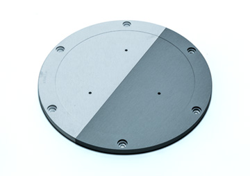
Comparison before and after anodizing process
Anodizing treatment is the anodic oxide coating treatment of aluminum.
Although this treatment is generally called “alumite treatment” in Japan, it is the same as “anodizing treatment”. This treatment is based on the technology to grow the oxide layer mainly through the electrolysis in a strong acid using the surface of the treated material as an anode to coat the aluminum surface with alumina.
Features
Our anodizing treatment is focused on vacuum components used in the process chamber of semiconductor and FPD (liquid crystal and organic EL) manufacturing equipment and performed in an environment where impurities contained in processing liquids and particles in blown air are controlled within the specifications required for vacuum components.
Microscopic Structure
Our anodized film has a microscopic structure with very few surface defects (blowholes and pinholes caused by impurities) suitable for semiconductor manufacturing processes.
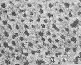
A photo of the surface of anodizing film for semiconductor manufacturing equipment components (400,000 magnifications)
Dedicated Production Lines for Semiconductor and Flat Panel Display Manufacturing Equipment
We can treat components of 450 mm in diameter for semiconductor manufacturing equipment and large-sized components for FPD manufacturing equipment.
The maximum workpiece sizes
Domestic production site (Saitama): 3,000 (Length) x 2,500 (Depth) x 600 (Width) mm
Chinese production site (Zhuhai): 4,000 (Length) x 3,400 (Depth) x 700 (Width) mm
※Including suspended and electrode fixture parts. => Details are to be discussed separately.
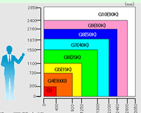
Suitable FPD sizes for each generation
Film Forming Specifications
Not only semi-hard but also hard films with a film thickness between 2 and 70 μm can be formed. In addition, we offer two types of sealing treatments for enhancing corrosion resistance: pressurization with steam (up to φ450 mm) and boiling with pure water. And the processing solutions can be selected from various types, such as sulfuric acid and oxalic acid according to the requirements.
Customizable Anodized Film
Along with changes in semiconductor and liquid crystal manufacturing processes, it is increasingly becoming difficult to use anodized films that could be used with no problem previously. We propose anodized films suitable for customers’ processes based on the evaluation of film thickness, hardness, and surface roughness using dedicated evaluation equipment according to their requirements. In addition, in mass production, we provide stable and reproducible anodized films using computerized automatic control and separate control tables.
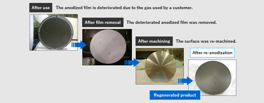
Regeneration Treatment Technology
Semiconductor and FPD manufacturing equipment components are very expensive. We can perform regeneration treatment in which various types of films applied to the components when customers put them in processes are removed, their surfaces are polished or machined again, and they are re-anodized to recover their performance having the same properties as those of new components. In addition, we can also perform mirror surface treatment for improving the flow of process gas as well as blasting process for improving soaking distribution in our plant. Chemically cleaning or anodizing products that went through mirror surface or blasting treatment provides regenerated products with minimum contamination and particles.