Applications
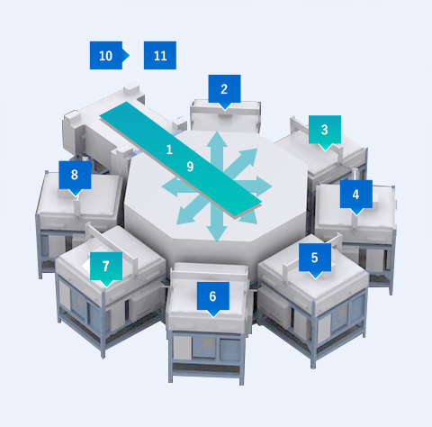
■:Process in which our parts are installed
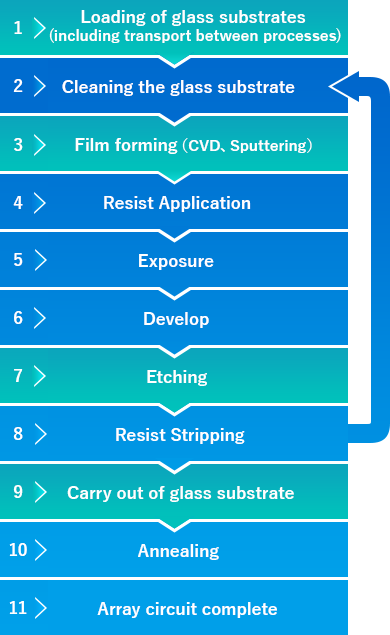
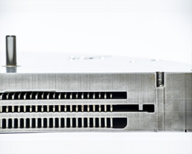
We offer mainly semiconductor device, FPD (liquid crystal and organic EL) substrate, and LED device manufacturing devices for a wide variety of processes. In particular, we have a long history of supplying metallic components, which went through various processes from machining to secondary processing, such as brazing and surface treatment, used in a vacuum chamber for film forming and etching processes. In addition, we also offer magnetic circuits that are used in a film forming process or linear transfer system.
| CVD |
It is one of vapor deposition method which forms thin film on the surface of substrate by chemical reaction. We are good at plasma CVD which excites atoms and molecules by plasma and parts used for MOCVD mainly used for manufacturing LEDs. |
| Sputtering |
Used to deposit metal films. It is used for film formation of TFT elements that control lighting of pixels of liquid crystal television. |
| Etching |
This is the process of corroding and removing the exposed thin film by exposure and development. OGF processing which is our proprietary technology characterized by high corrosion resistance is utilized. |
| Transport |
Our magnetic application technology is utilized for the mechanism to transport the glass substrate to the chamber of the next process. |
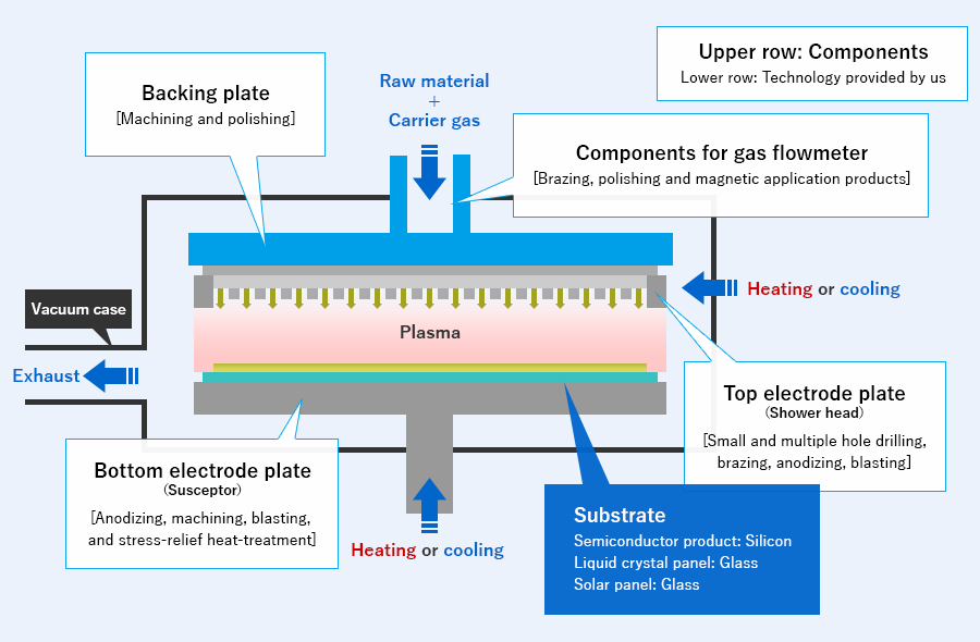
The technologies we provide for CVD device components
Advantages of Our Equipment Component Business
We provide functions required for components to materials
For over 30 years, we have been procuring materials and supplying components that went through the machining, jointing, and surface treatment processes to the semiconductor manufacturing equipment industry where high quality is required.
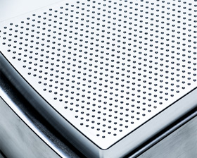
Precise machining technologies such as small and multiple hole drilling
Precise jointing technologies that achieve the air tightness on the Helium Level
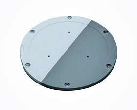
Surface treatment technologies that treat thin films to large components
We propose designs that suit the environment where they are used.
We can select materials and propose designs that are suitable for the use environment such as temperature and atmosphere.
We propose jointing methods that realize 3D structure and the quality of anodize that meets your demand.
We have a production plant in China where semiconductor and FPD markets are growing rapidly.
Our production plant in China, Zhuhai, has the same equipment as that of our Saitama plant.
And it is equipped with facilities for machining and treating large components. The components are mass-produced in our production base in Zhuhai, China and distributed to different companies in China and Southeast Asia after manufacturing processes are designed and verified in our domestic production bases.
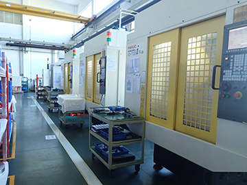
Machining equipment in China Plant
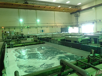
Surface treatment equipment in China Plant
We manage the traceability of each component.
Our Saitama plant performs and manages various processes ranging from machining to secondary processing, such as jointing and surface treatment, in a consistent way to realize the management of traceability on a single component basis. In addition, it introduced the statistical process control (SPC) method to enhance its quality control.
We have clean rooms.
Our production plants in Japan and China have clean rooms that assemble and pack precision-machined and cleaned
components under clean environment.
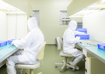
Clean room in Saitama Plant
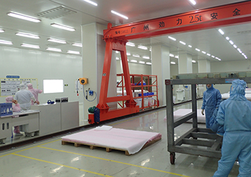
Clean room in China Plant